Lecture 1
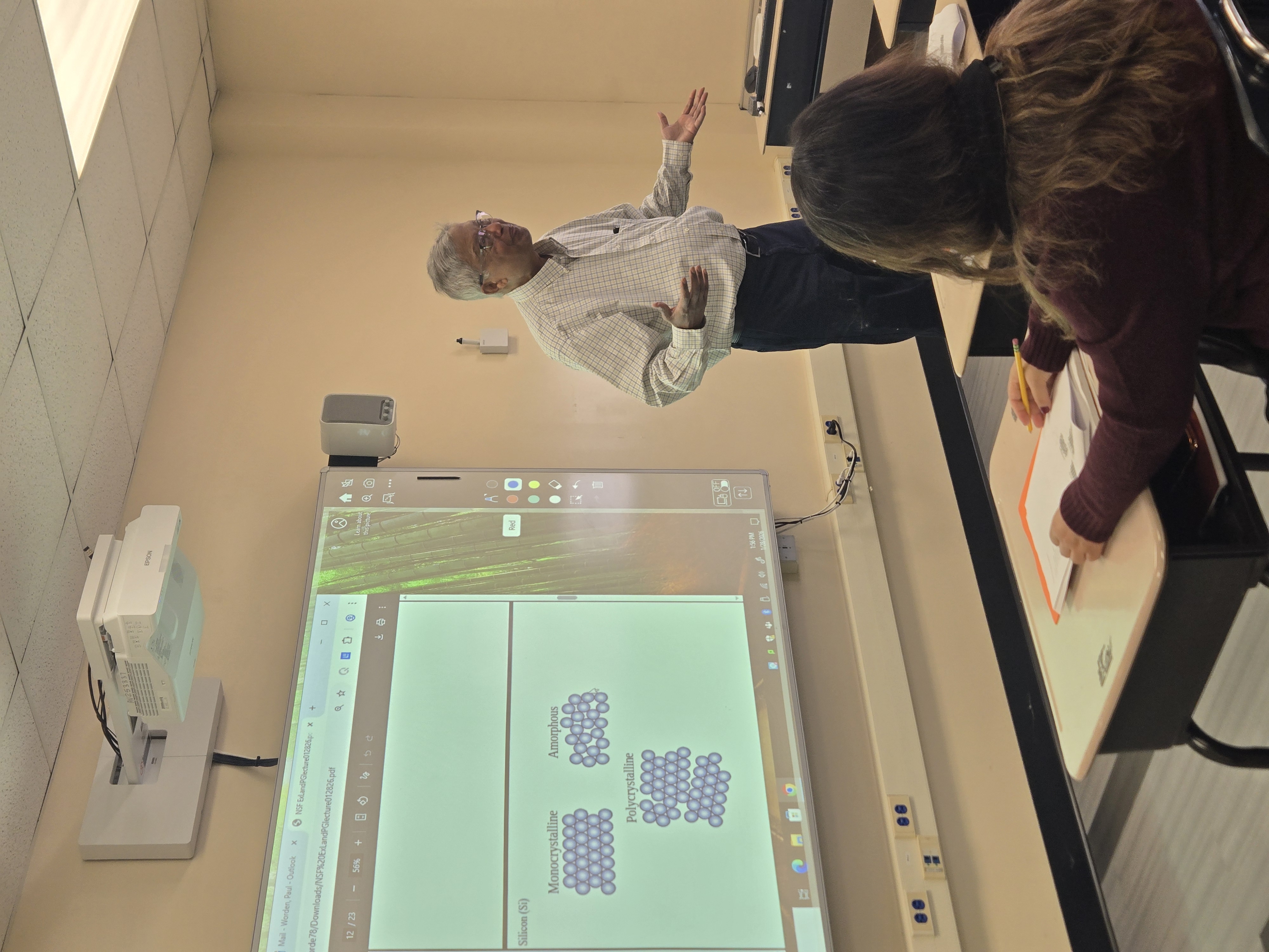
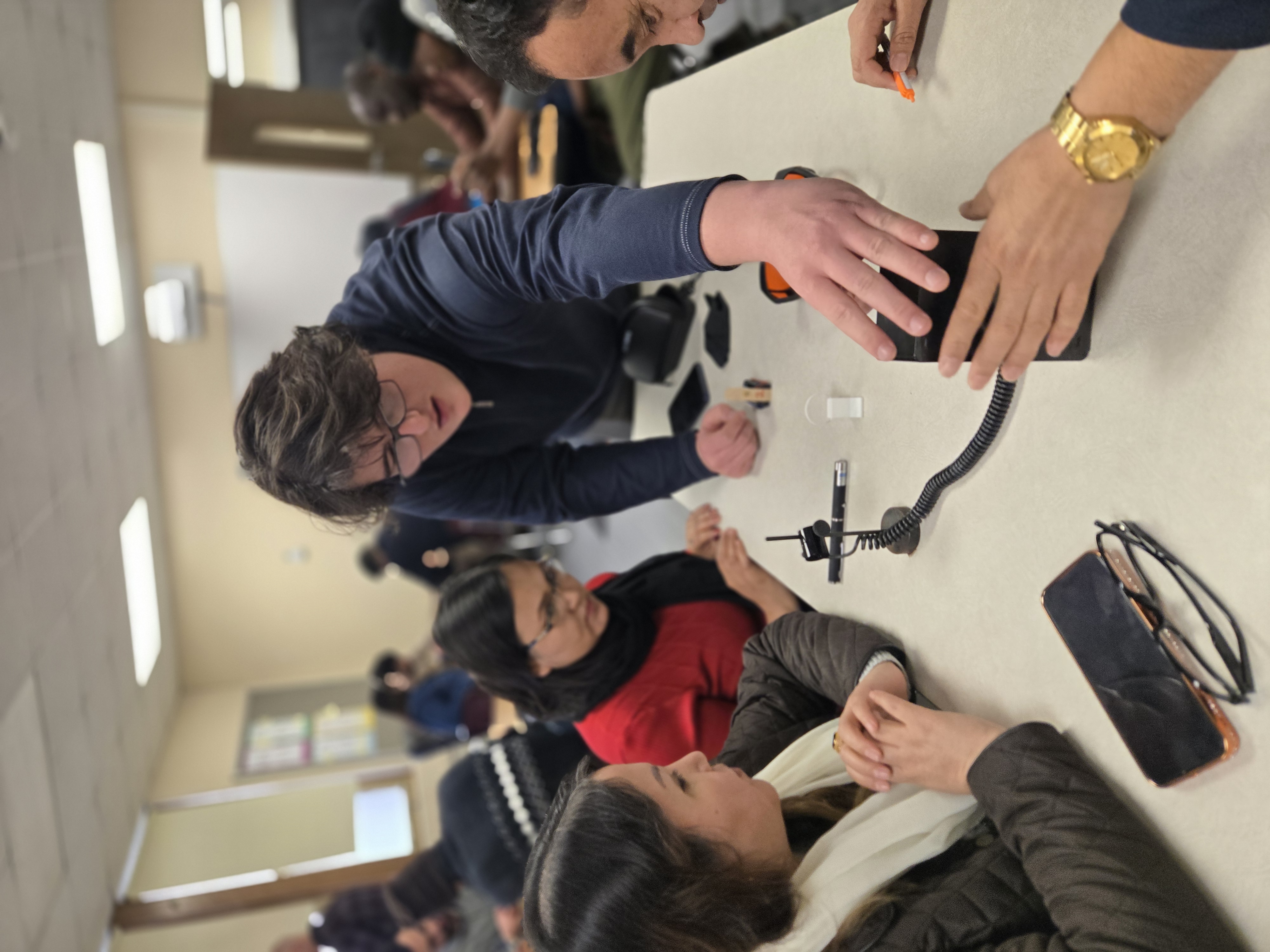
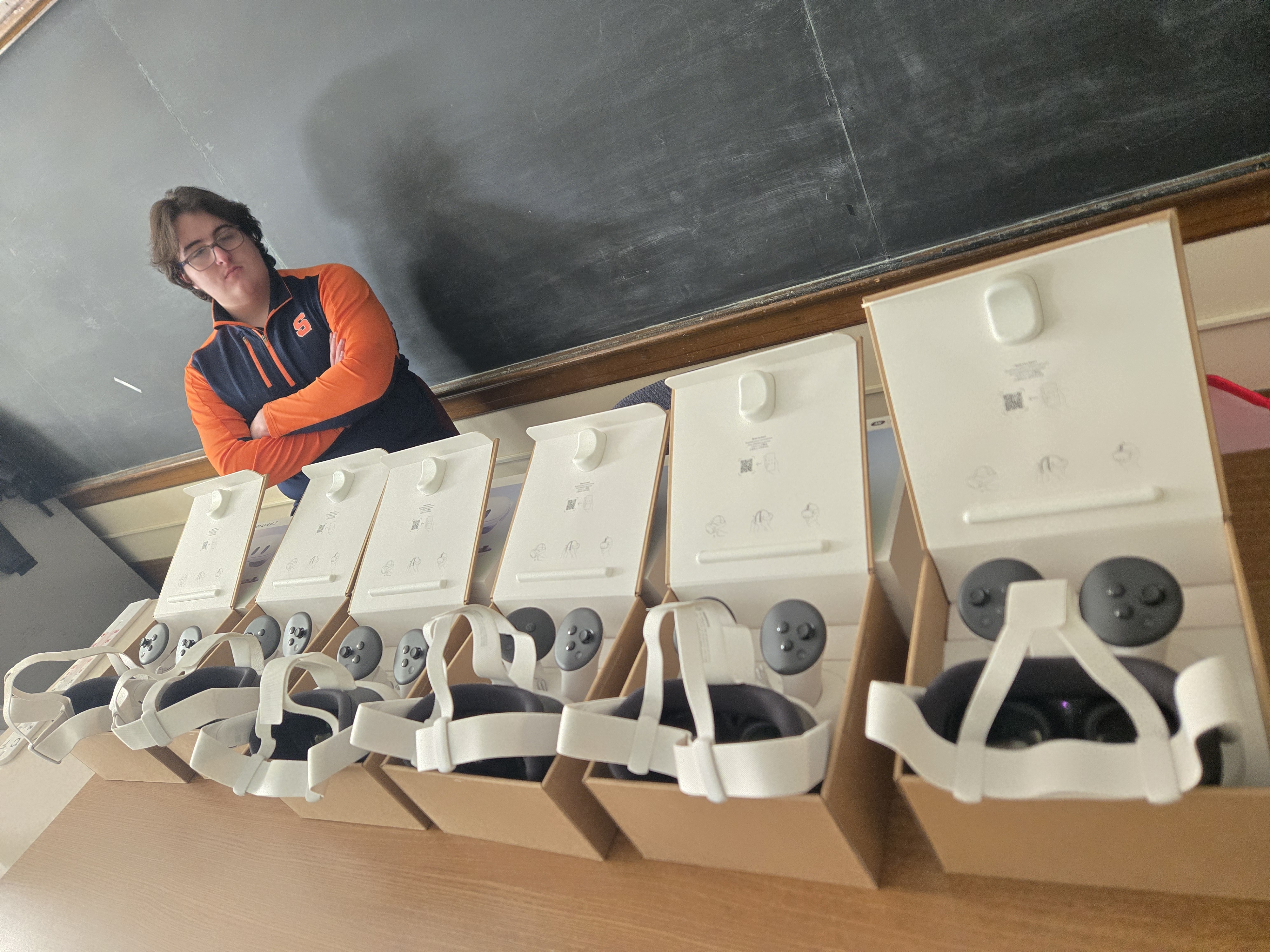
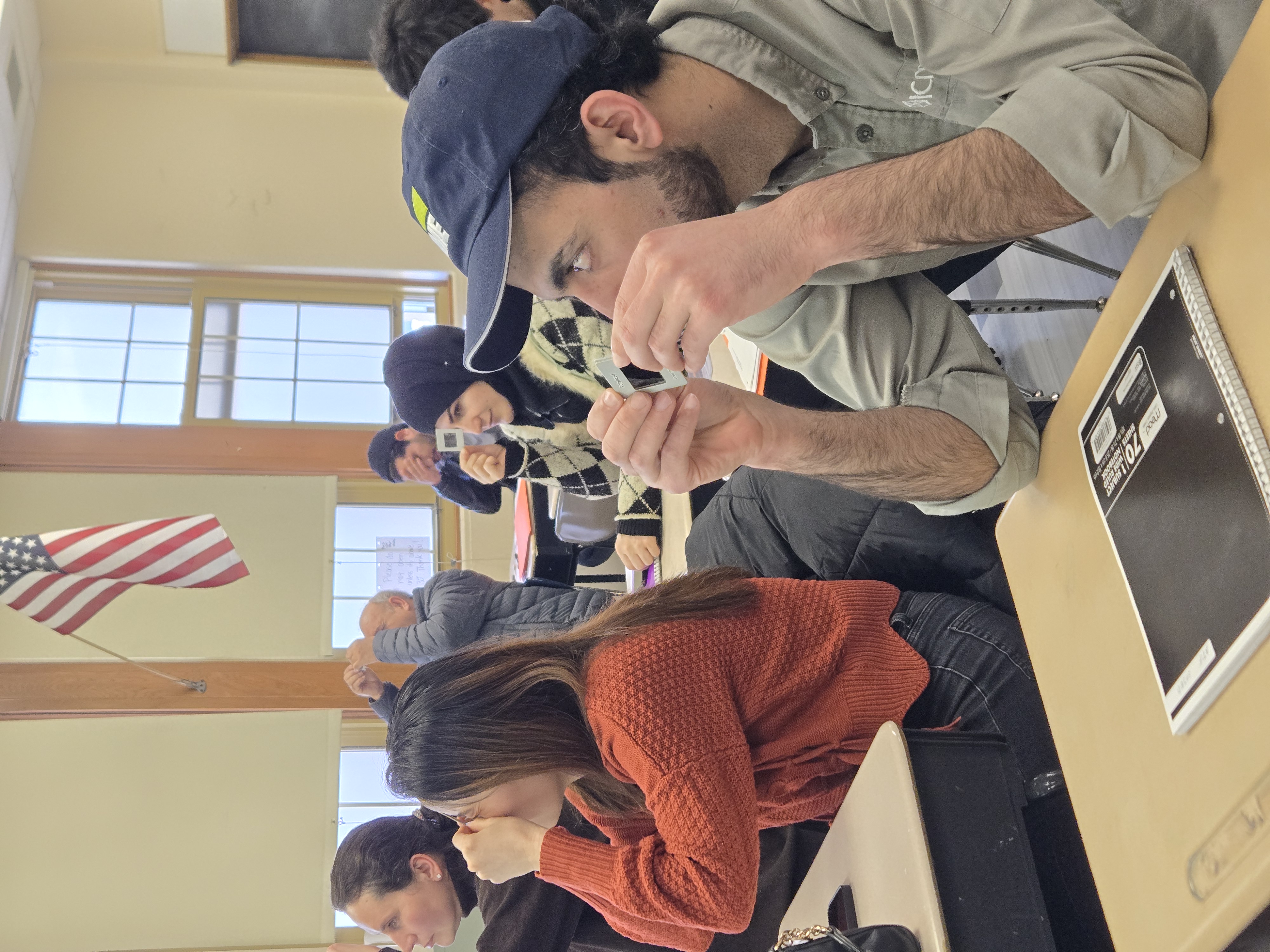
Highlights from Q-SUCCEED lectures, workshops, and field trips.
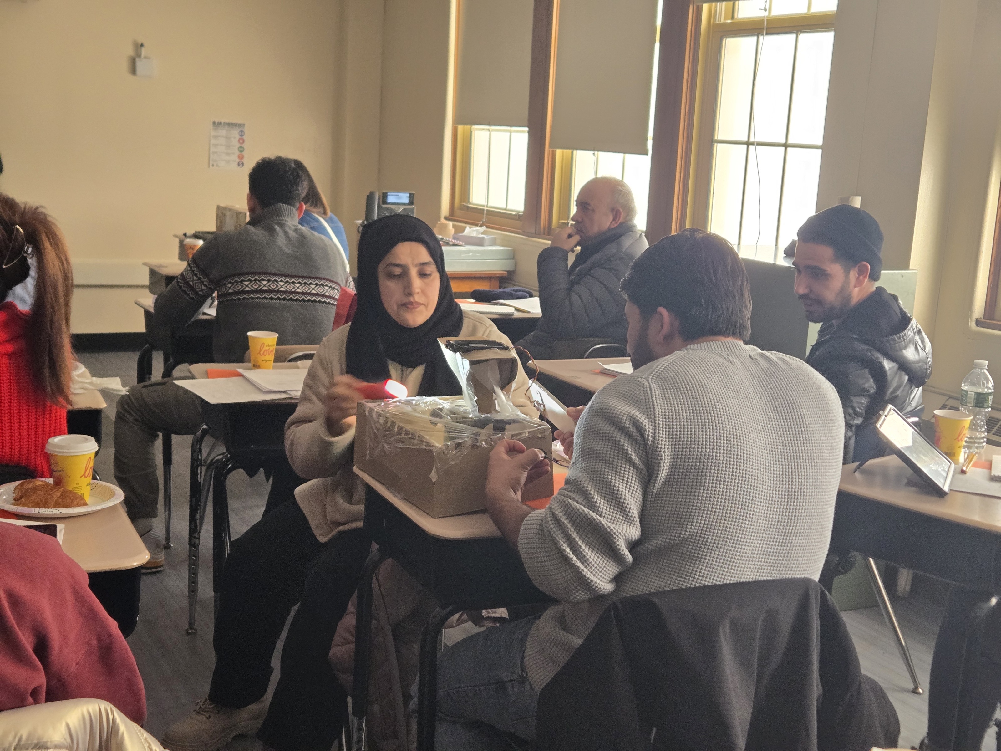
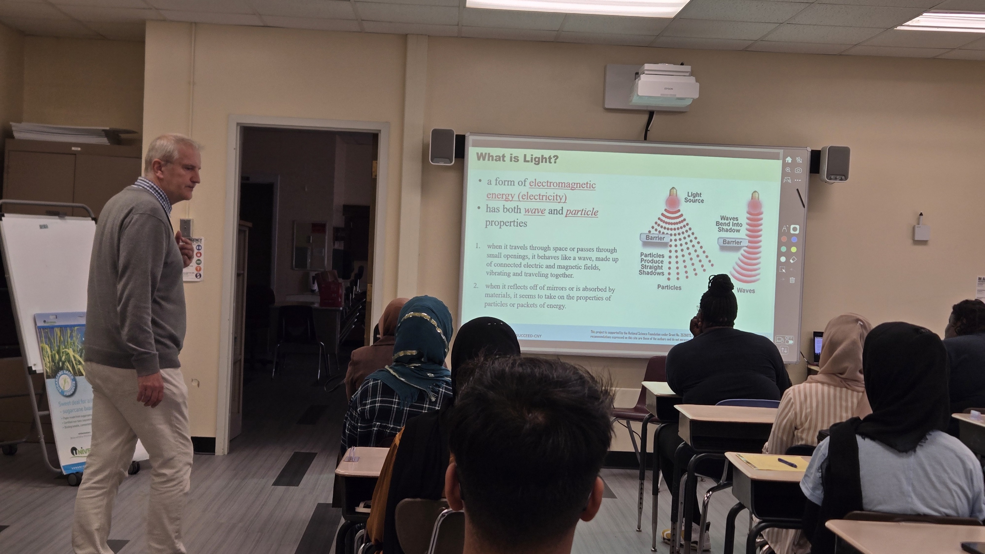
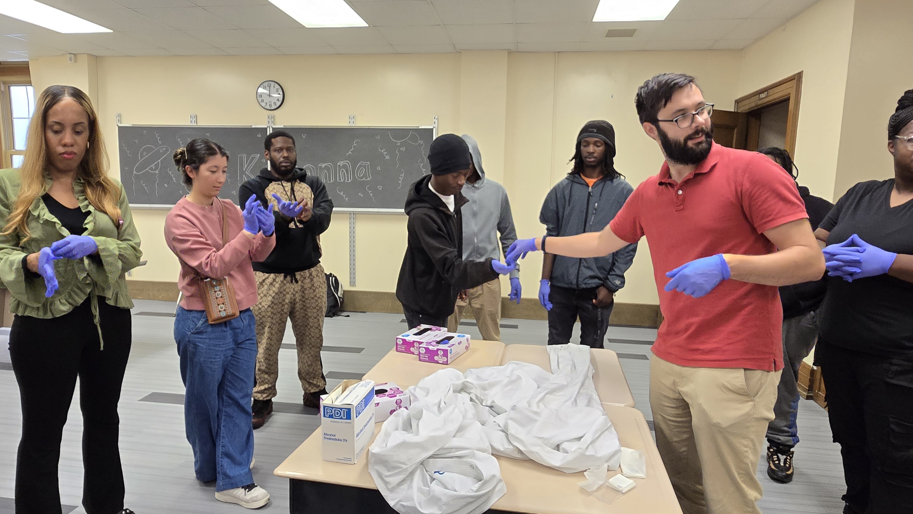
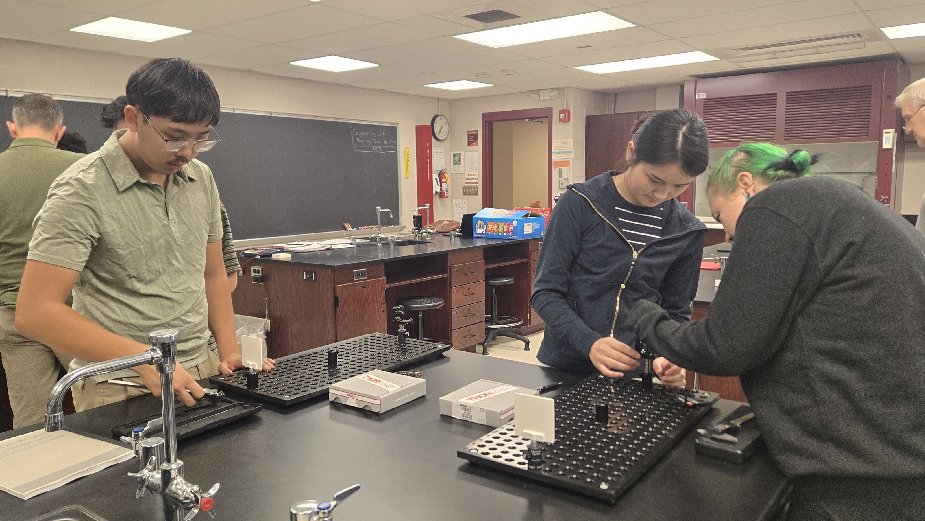
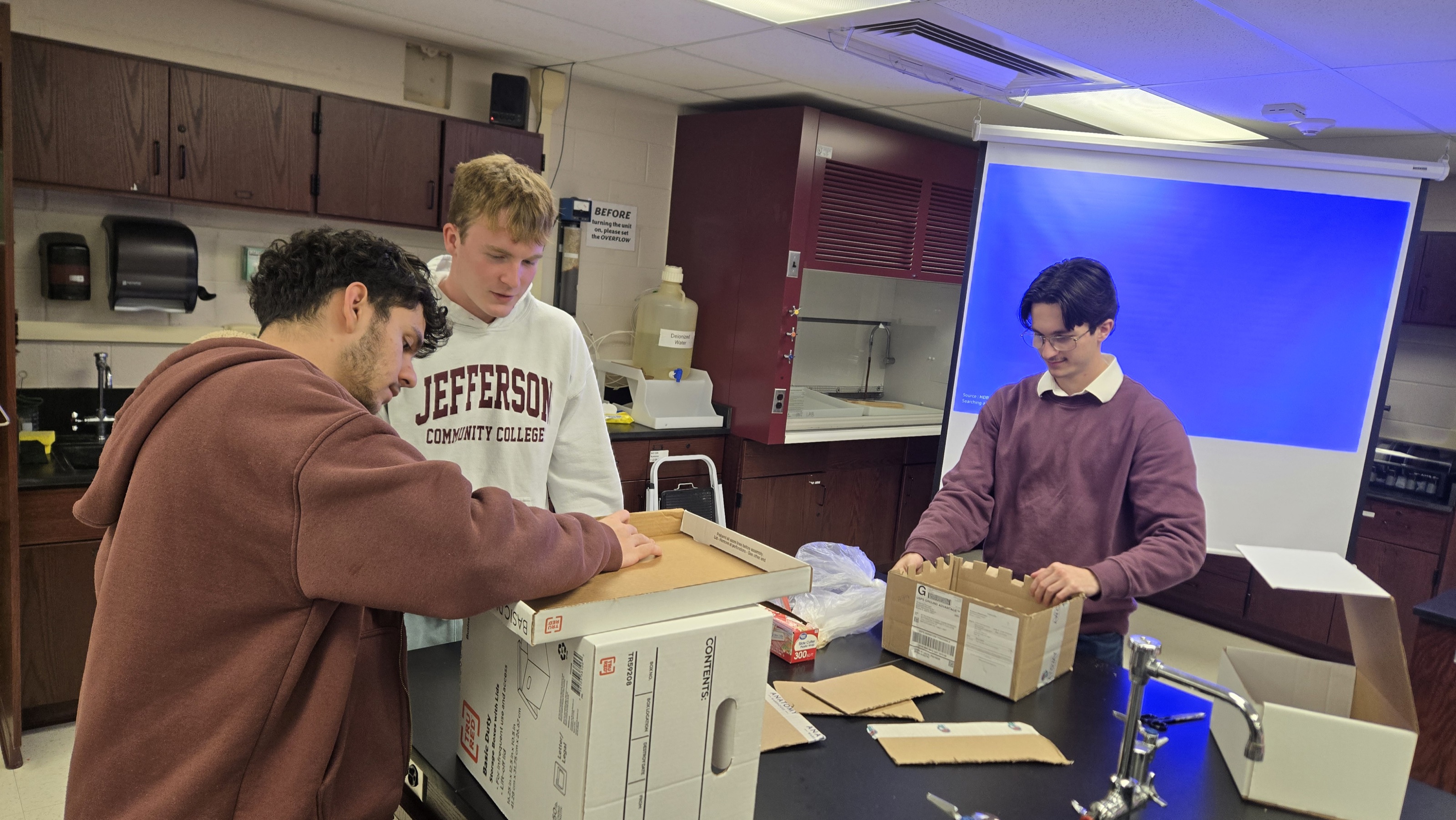
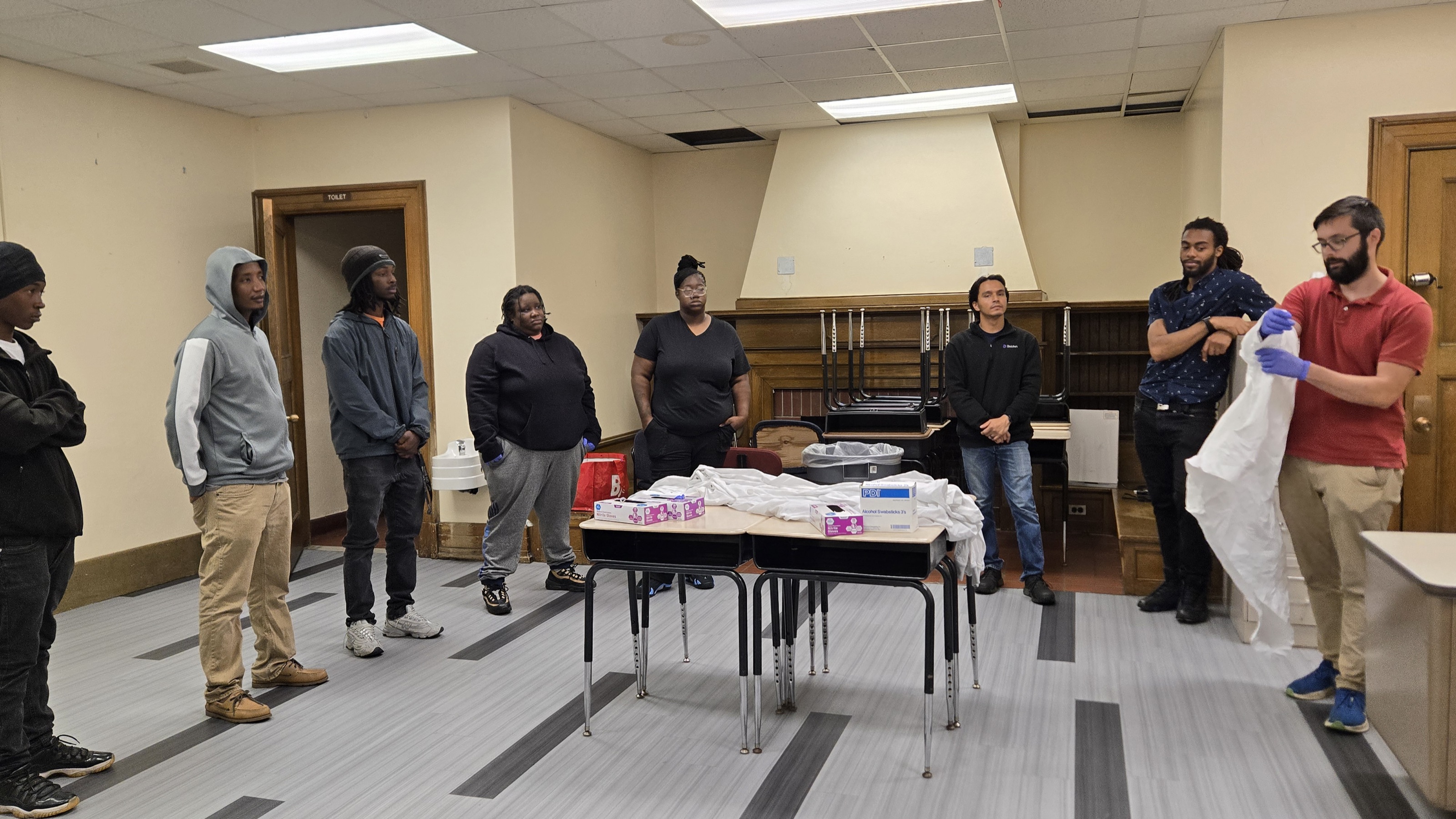
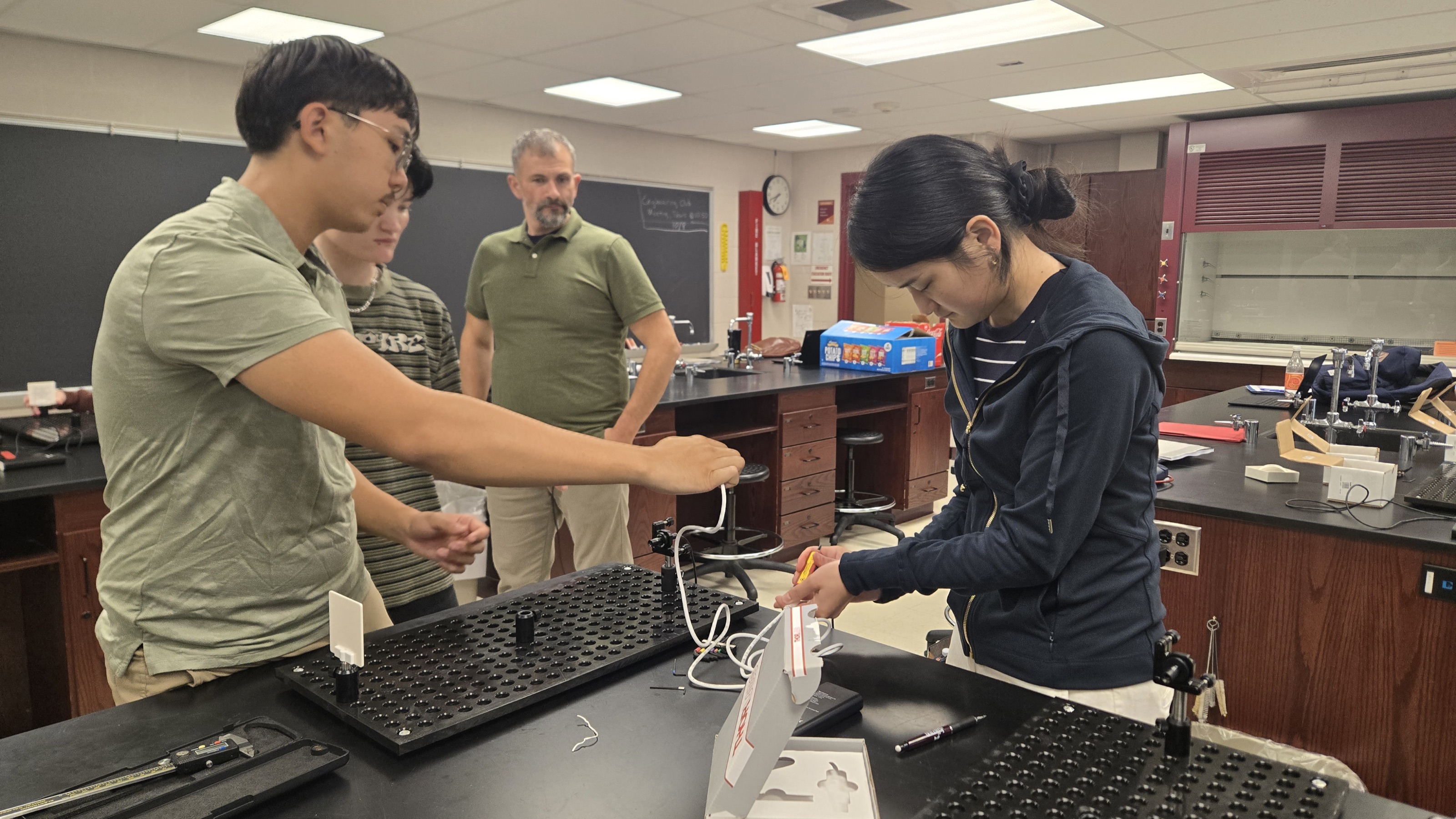
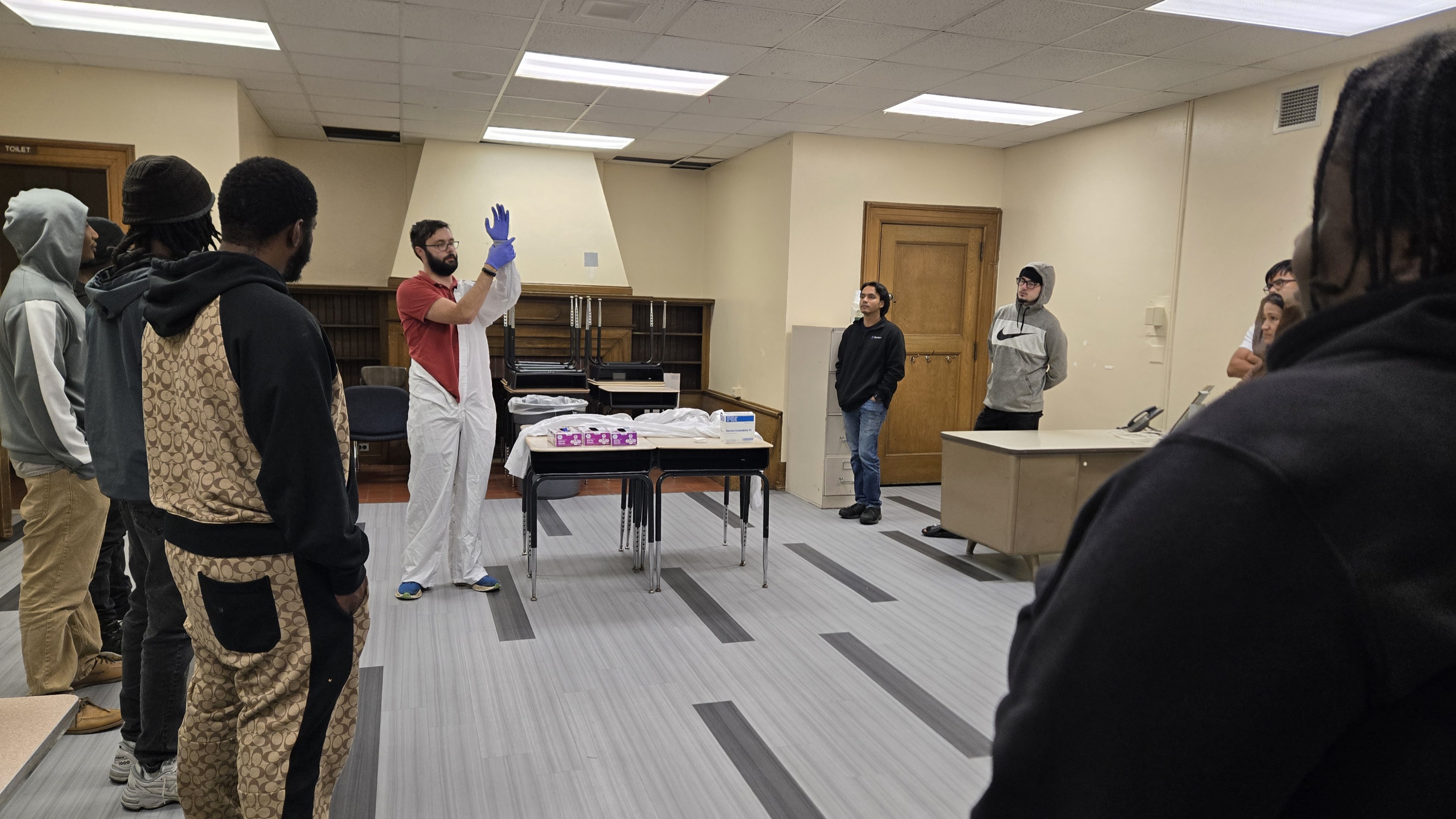
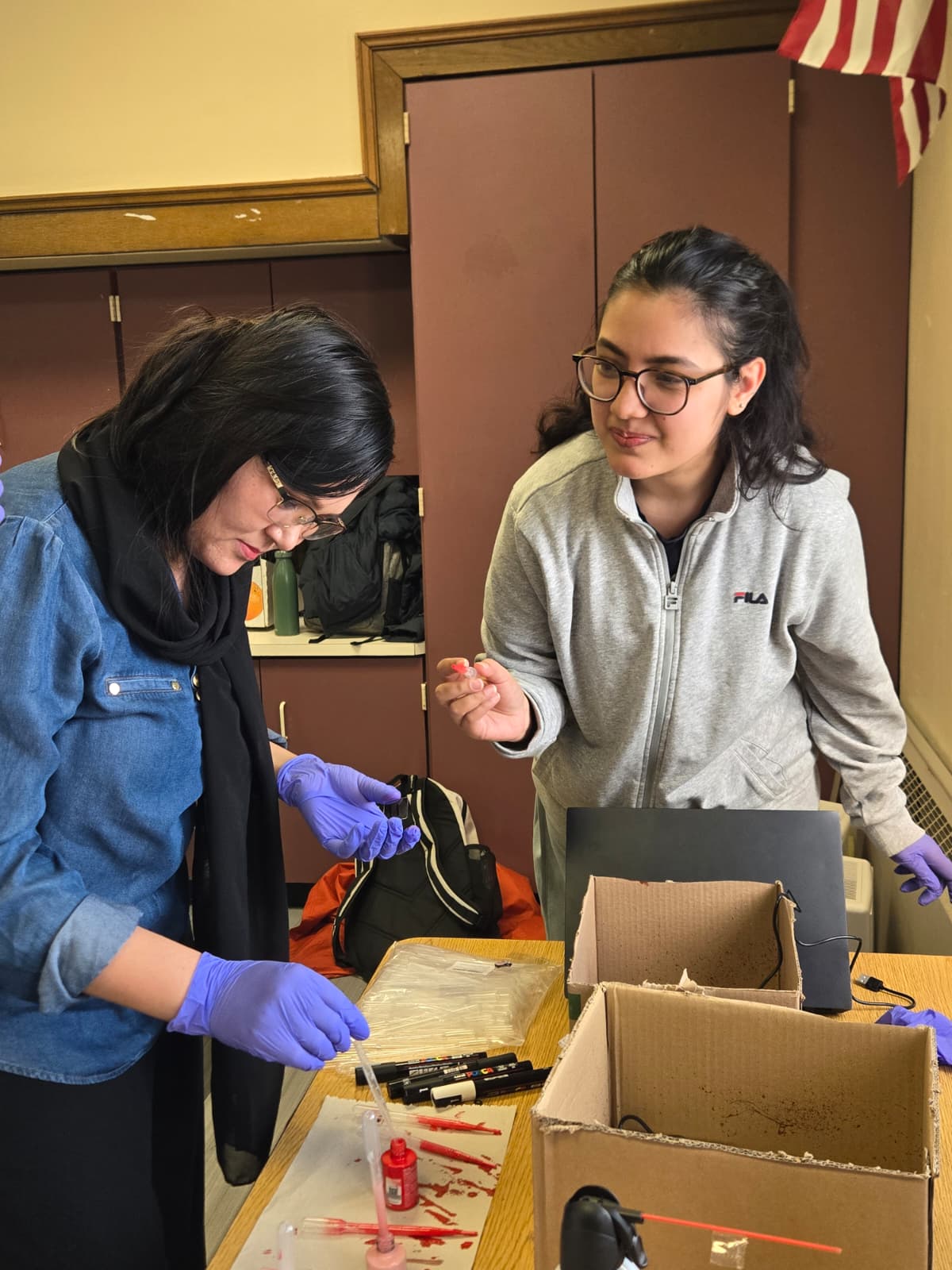
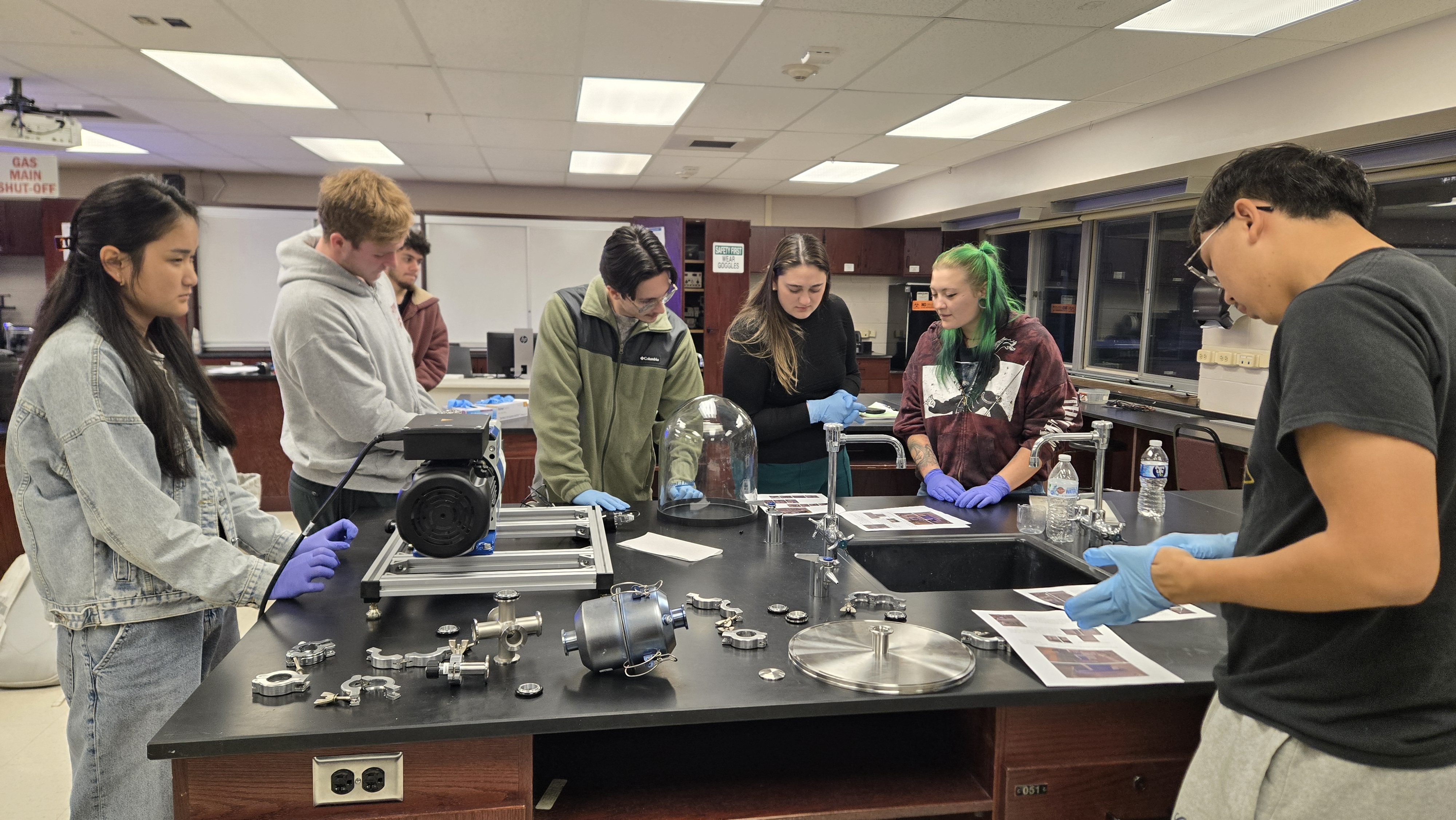
The Weekly Lecture series introduce participants to semiconductor and quantum technologies through a semester-long series of sessions, where every lecture is followed by hands-on activities to reinforce learning. Starting with an orientation, participants progressively explore vacuum processes, plasma processing, photolithography, and gold plating on the semiconductor side, then transition into laser-based measurements, quantum optics, the double-slit experiment, and quantum cryptography. This lecture series was conducted in Spring 2026 with the first cohort of 20 participants from the Syracuse City School District Adult Education Center. We extend a special thanks to Dr. John P. Iorio, Director of the SCSD Adult Education Department, as well as SCSD Adult Education Team members Janet Staub, Paul Worden, and Jasenko Mondom, for their continued support of the Q-SUCCEED-CNY program.
.jpeg)
.jpeg)
.jpeg)
A hands-on visit to one of the nation's leading nanofabrication facilities experiencing cleanroom culture, wafer processing, and the precision behind microchip manufacturing.
.jpeg)
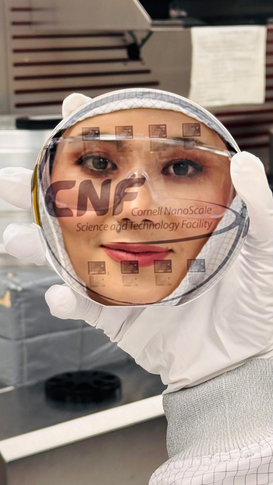
Participants visited the Cornell NanoScale Science and Technology Facility. One group toured the cleanroom to observe wafer processing and photomask alignment up close, while the other explored the Cornell campus.
.jpeg)
.jpeg)
.jpeg)
.jpeg)
.jpeg)
.jpeg)
.jpeg)
.jpeg)
.jpeg)
.jpeg)
.jpeg)
.jpeg)
.jpeg)
.jpeg)
.jpeg)
Trip Description
Participants toured the Cornell NanoScale Science and Technology Facility (CNF), guided by Tom through the cleanroom. The group observed the full semiconductor fabrication process — from wafer preparation and spin-coating of photoresist, to UV exposure through photomasks that transfer intricate circuit patterns onto silicon. Inside the yellow-lit lithography bay, participants saw firsthand how photomasks act as stencils, projecting nanoscale designs onto coated wafers with precise alignment under microscope stations.
Participants suited up in full cleanroom gowns, gloves, and hairnets before entering the controlled environment, learning about the strict contamination protocols that keep particle counts near zero. They observed technicians handling wafers, operating deposition and etching equipment, and inspecting patterned chips through the CNF's transparent wafer holders. Meanwhile, a second group enjoyed a campus tour, taking in Cornell's iconic clock tower and grounds. The visit gave participants a real sense of the precision, discipline, and career opportunities inside a working nanofabrication facility.
From Thomas Pennell — Process Integration Specialist & Workforce Development Program Manager at Cornell Nanoscale Facility
The Cornell NanoScale Science and Technology Facility (CNF) hosted adult learners from Syracuse University's Q-SUCCEED-CNY program led by Mo Hasanovic. These students were new to the United States and the program gave them the opportunity to explore careers in the semiconductor industry in the classroom, in VR and finally in person at CNF.
I took the students through the lab in groups and showed the steps in fabricating a device in real time! When it came time for inspection, they were blown away at a 200 μm wide Cornell University logo under the microscope. They were awestruck when I played a video on my cell phone under a microscope and they got to see the micro-LEDs changing color in front of their eyes.
What an amazing group of people! I am so proud to take part in a program like this that embraces people from Afghanistan, the Republic of Congo and Cuba and shows them the best of what our country has to offer!
Side note: we have cleanroom suits that comfortably fit a person that is 7' tall and has size 15 shoes!
📷 Trip Photos
.jpeg)
.jpeg)
.jpg)
.jpeg)
.jpeg)
.jpeg)
.jpeg)
.jpeg)
Our intensive five-day workshop from April 27 – May 1
.jpeg) April 27 – May 1, 2026
April 27 – May 1, 2026
Lectures, labs, a CNF cleanroom field trip, job prep, and industry networking in 5 days.
.jpeg)
.jpeg)
.jpeg)
.jpeg)
.jpeg)
.jpeg)
.jpeg)
.jpeg)
.jpeg)
.jpeg)
.jpeg)
.jpeg)
.jpeg)
.jpeg)
.jpeg)
.jpeg)
.jpeg)
.jpeg)
.jpeg)
.jpeg)
.jpeg)
.jpeg)
.jpeg)
.jpeg)
.jpeg)
.jpeg)
.jpeg)
.jpeg)
.jpeg)
Workshop Overview
The last five days condensed the full Q-SUCCEED-CNY experience into an intensive bootcamp. Participants attended daily lectures and lab activities covering semiconductor fundamentals and quantum technologies, led by instructors Mo, Ethan, and Alex J.
On Monday and Tuesday, participants dove into foundational lectures, semiconductor and quantum lab activities, a job preparedness workshop with Jeffrey, and TDO sessions. Wednesday featured the highlight of the week - a field trip to the Cornell NanoScale Science and Technology Facility (CNF) in Ithaca, where participants toured the cleanroom and observed real wafer processing. Thursday brought more advanced quantum lab activities with lectures from Professor Ethan and a session with Ben from OCC. The week culminated on Friday with lecture from Dr. Alex K. Jones and session from SU College of Professional Studies, followed by a graduation ceremony celebrating the participants' achievements.
Additional activities throughout the week included an SU campus tour. Industry partners were involved, connecting participants directly to hiring pathways in the tech field.
📅Schedule
Monday, April 27
Lecture (Mo) · Coffee Break · TTM Session · MACNY Visit · Lunch · Semiconductor & Quantum Lab Activity)
Tuesday, April 28
Lecture (Ethan) · Job Preparedness Workshop (Jeffrey) · Lunch · TDO Session · Coffee Break · Lecture (Mo)
Wednesday, April 29 — Field Trip
Full-day field trip to Cornell NanoScale Science & Technology Facility (CNF) in Ithaca — cleanroom tour and campus exploration
Thursday, April 30
Semiconductor & Quantum Lab Activity · Lunch · Lecture (Ethan) · Coffee Break · Session with Ben (OCC)
Friday, May 1 — Graduation
Session with Alex J · SU College of Professional Studies· Lunch · Graduation Ceremony 🎓
📷 Workshop Photos
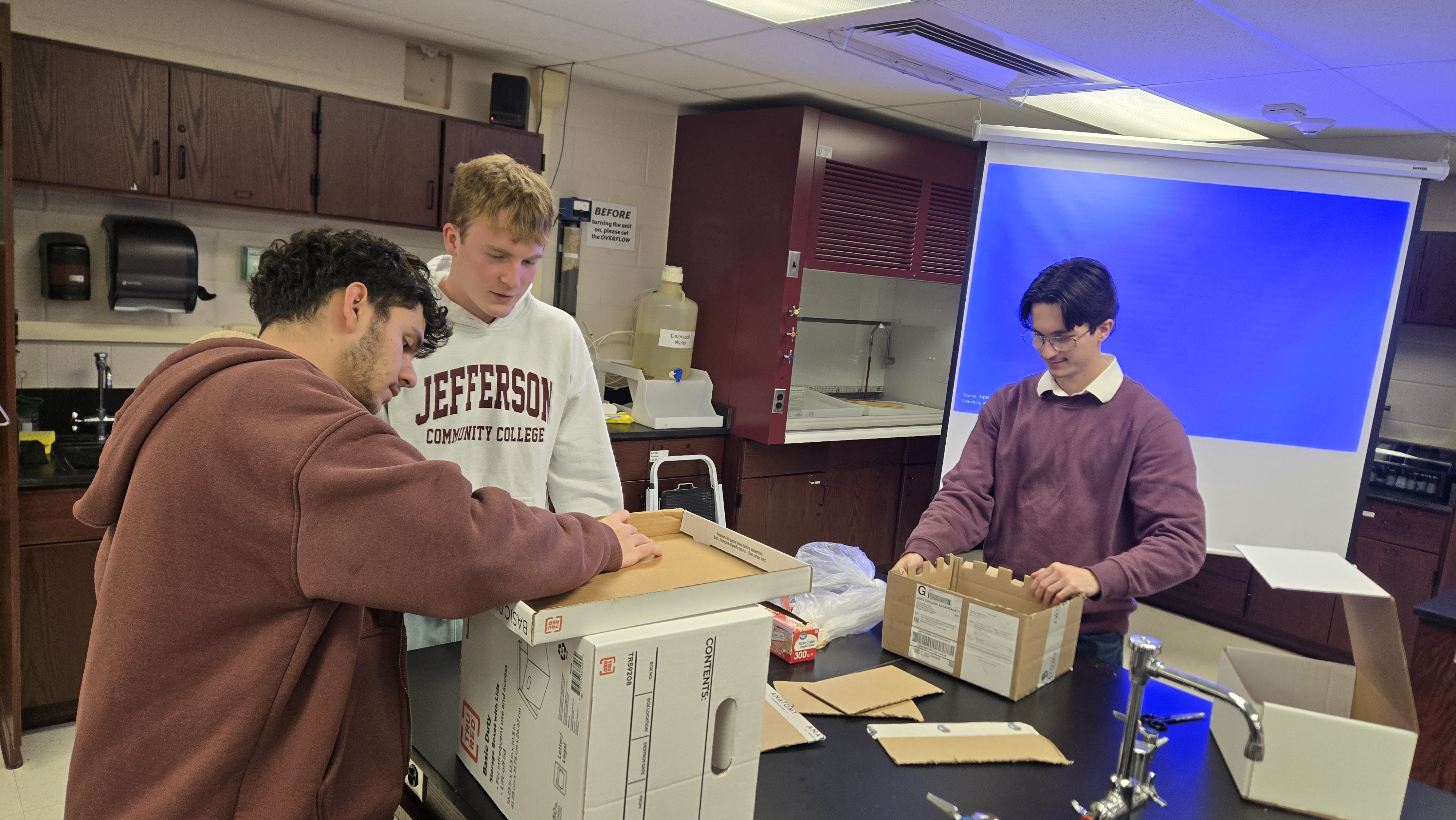
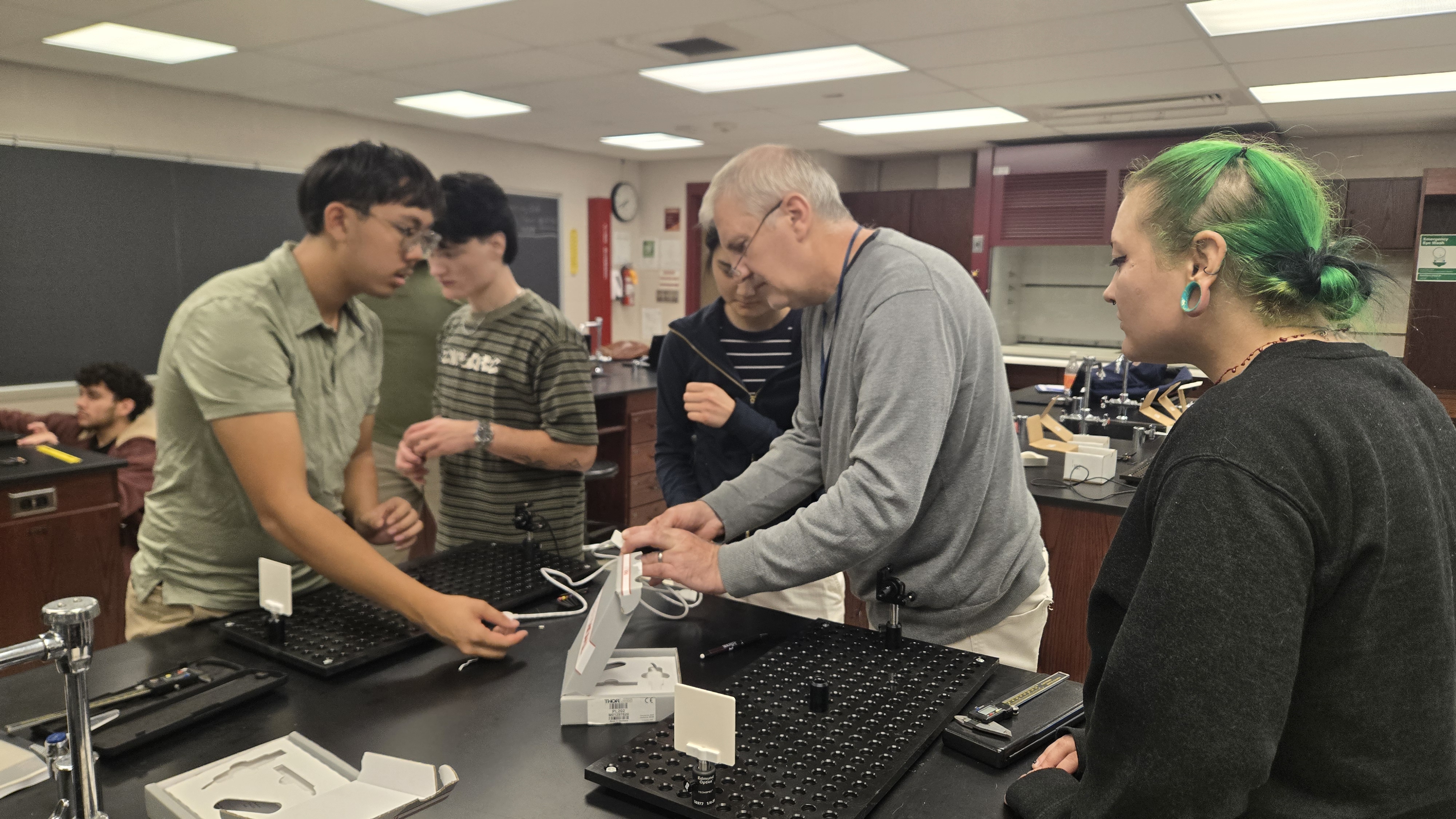
The Weekly Lecture series introduce participants to semiconductor and quantum technologies through a semester-long series of sessions, where every lecture is followed by hands-on activities to reinforce learning. Starting with an orientation, participants progressively explore vacuum processes, plasma processing, photolithography, and gold plating on the semiconductor side, then transition into laser-based measurements, quantum optics, the double-slit experiment, and quantum cryptography. This lecture series is currently being delivered to the Fall 2026 cohort. We extend a special thanks to Dr. John P. Iorio, Director of the SCSD Adult Education Department, SCSD Adult Education team members Janet Staub, Paul Worden, and Jasenko Mondom, and, from Jubilee Homes, Cherylene Billue(Director of Workforce Initiatives), and Madea Holman(Program Manager), for their continued support of the Q-SUCCEED-CNY program.
The images below are stock illustrations of each topic. Fall 2026 session photos and dates will replace them as the semester progresses.


Field trip details for Fall 2026 will be announced as the semester progresses.
Session Description
📷 Session Photos

